This timeline features Premodern example of nanotechnology, as well as Modern Era discoveries and milestones in the field of nanotechnology.
Early examples of nanostructured materials were based on craftsmens empirical understanding and manipulation of materials. Use of high heat was one common step in their processes to produce these materials with novel properties.
The Lycurgus Cup at the British Museum, lit from the outside (left) and from the inside (right)
4th Century: The Lycurgus Cup (Rome) is an example of dichroic glass; colloidal gold and silver in the glass allow it to look opaque green when lit from outside but translucent red when light shines through the inside. (Images at left.)
9th-17th Centuries: Glowing, glittering luster ceramic glazes used in the Islamic world, and later in Europe, contained silver or copper or other metallic nanoparticles. (Image at right.)
6th-15th Centuries: Vibrant stained glass windows in European cathedrals owed their rich colors to nanoparticles of gold chloride and other metal oxides and chlorides; gold nanoparticles also acted as photocatalytic air purifiers. (Image at left.)
13th-18th Centuries: Damascus saber blades contained carbon nanotubes and cementite nanowiresan ultrahigh-carbon steel formulation that gave them strength, resilience, the ability to hold a keen edge, and a visible moir pattern in the steel that give the blades their name. (Images below.)
These are based on increasingly sophisticated scientific understanding and instrumentation, as well as experimentation.
1857: Michael Faraday discovered colloidal ruby gold, demonstrating that nanostructured gold under certain lighting conditions produces different-colored solutions.
1936: Erwin Mller, working at Siemens Research Laboratory, invented the field emission microscope, allowing near-atomic-resolution images of materials.
1947: John Bardeen, William Shockley, and Walter Brattain at Bell Labs discovered the semiconductor transistor and greatly expanded scientific knowledge of semiconductor interfaces, laying the foundation for electronic devices and the Information Age.
1950: Victor La Mer and Robert Dinegar developed the theory and a process for growing monodisperse colloidal materials. Controlled ability to fabricate colloids enables myriad industrial uses such as specialized papers, paints, and thin films, even dialysis treatments.
1951: Erwin Mller pioneered the field ion microscope, a means to image the arrangement of atoms at the surface of a sharp metal tip; he first imaged tungsten atoms.
1956: Arthur von Hippel at MIT introduced many concepts ofand coined the termmolecular engineering as applied to dielectrics, ferroelectrics, and piezoelectrics
1958: Jack Kilby of Texas Instruments originated the concept of, designed, and built the first integrated circuit, for which he received the Nobel Prize in 2000. (Image at left.)
1959: Richard Feynman of the California Institute of Technology gave what is considered to be the first lecture on technology and engineering at the atomic scale, "There's Plenty of Room at the Bottom" at an American Physical Society meeting at Caltech. (Image at right.)
1965: Intel co-founder Gordon Moore described in Electronics magazine several trends he foresaw in the field of electronics. One trend now known as Moores Law, described the density of transistors on an integrated chip (IC) doubling every 12 months (later amended to every 2 years). Moore also saw chip sizes and costs shrinking with their growing functionalitywith a transformational effect on the ways people live and work. That the basic trend Moore envisioned has continued for 50 years is to a large extent due to the semiconductor industrys increasing reliance on nanotechnology as ICs and transistors have approached atomic dimensions.1974: Tokyo Science University Professor Norio Taniguchi coined the term nanotechnology to describe precision machining of materials to within atomic-scale dimensional tolerances. (See graph at left.)
1981: Gerd Binnig and Heinrich Rohrer at IBMs Zurich lab invented the scanning tunneling microscope, allowing scientists to "see" (create direct spatial images of) individual atoms for the first time. Binnig and Rohrer won the Nobel Prize for this discovery in 1986.
1981: Russias Alexei Ekimov discovered nanocrystalline, semiconducting quantum dots in a glass matrix and conducted pioneering studies of their electronic and optical properties.
1985: Rice University researchers Harold Kroto, Sean OBrien, Robert Curl, and Richard Smalley discovered the Buckminsterfullerene (C60), more commonly known as the buckyball, which is a molecule resembling a soccer ball in shape and composed entirely of carbon, as are graphite and diamond. The team was awarded the 1996 Nobel Prize in Chemistry for their roles in this discovery and that of the fullerene class of molecules more generally. (Artist's rendering at right.)
1985: Bell Labss Louis Brus discovered colloidal semiconductor nanocrystals (quantum dots), for which he shared the 2008 Kavli Prize in Nanotechnology.
1986: Gerd Binnig, Calvin Quate, and Christoph Gerber invented the atomic force microscope, which has the capability to view, measure, and manipulate materials down to fractions of a nanometer in size, including measurement of various forces intrinsic to nanomaterials.
1989:Don Eigler and Erhard Schweizer at IBM's Almaden Research Center manipulated 35 individual xenon atoms to spell out the IBM logo. This demonstration of the ability to precisely manipulate atoms ushered in the applied use of nanotechnology. (Image at left.)
1990s: Early nanotechnology companies began to operate, e.g., Nanophase Technologies in 1989, Helix Energy Solutions Group in 1990, Zyvex in 1997, Nano-Tex in 1998.
1991: Sumio Iijima of NEC is credited with discovering the carbon nanotube (CNT), although there were early observations of tubular carbon structures by others as well. Iijima shared the Kavli Prize in Nanoscience in 2008 for this advance and other advances in the field. CNTs, like buckyballs, are entirely composed of carbon, but in a tubular shape. They exhibit extraordinary properties in terms of strength, electrical and thermal conductivity, among others. (Image below.)
1992: C.T. Kresge and colleagues at Mobil Oil discovered the nanostructured catalytic materials MCM-41 and MCM-48, now used heavily in refining crude oil as well as for drug delivery, water treatment, and other varied applications.
1993: Moungi Bawendi of MIT invented a method for controlled synthesis of nanocrystals (quantum dots), paving the way for applications ranging from computing to biology to high-efficiency photovoltaics and lighting. Within the next several years, work by other researchers such as Louis Brus and Chris Murray also contributed methods for synthesizing quantum dots.
1998: The Interagency Working Group on Nanotechnology (IWGN) was formed under the National Science and Technology Council to investigate the state of the art in nanoscale science and technology and to forecast possible future developments. The IWGNs study and report, Nanotechnology Research Directions: Vision for the Next Decade (1999) defined the vision for and led directly to formation of the U.S. National Nanotechnology Initiative in 2000.
1999: Cornell University researchers Wilson Ho and Hyojune Lee probed secrets of chemical bonding by assembling a molecule [iron carbonyl Fe(CO)2] from constituent components [iron (Fe) and carbon monoxide (CO)] with a scanning tunneling microscope. (Image at left.)
1999: Chad Mirkin at Northwestern University invented dip-pen nanolithography (DPN), leading to manufacturable, reproducible writing of electronic circuits as well as patterning of biomaterials for cell biology research, nanoencryption, and other applications. (Image below right.)
1999early 2000s: Consumer products making use of nanotechnology began appearing in the marketplace, including lightweight nanotechnology-enabled automobile bumpers that resist denting and scratching, golf balls that fly straighter, tennis rackets that are stiffer (therefore, the ball rebounds faster), baseball bats with better flex and "kick," nano-silver antibacterial socks, clear sunscreens, wrinkle- and stain-resistant clothing, deep-penetrating therapeutic cosmetics, scratch-resistant glass coatings, faster-recharging batteries for cordless electric tools, and improved displays for televisions, cell phones, and digital cameras.
2000: President Clinton launched the National Nanotechnology Initiative (NNI) to coordinate Federal R&D efforts and promote U.S. competitiveness in nanotechnology. Congress funded the NNI for the first time in FY2001. The NSET Subcommittee of the NSTC was designated as the interagency group responsible for coordinating the NNI.
2003: Congress enacted the 21st Century Nanotechnology Research and Development Act (P.L. 108-153). The act provided a statutory foundation for the NNI, established programs, assigned agency responsibilities, authorized funding levels, and promoted research to address key issues.
2003: Naomi Halas, Jennifer West, Rebekah Drezek, and Renata Pasqualin at Rice University developed gold nanoshells, which when tuned in size to absorb near-infrared light, serve as a platform for the integrated discovery, diagnosis, and treatment of breast cancer without invasive biopsies, surgery, or systemically destructive radiation or chemotherapy.2004: The European Commission adopted the Communication Towards a European Strategy for Nanotechnology, COM(2004) 338, which proposed institutionalizing European nanoscience and nanotechnology R&D efforts within an integrated and responsible strategy, and which spurred European action plans and ongoing funding for nanotechnology R&D. (Image at left.)
2004: Britains Royal Society and the Royal Academy of Engineering published Nanoscience and Nanotechnologies: Opportunities and Uncertainties advocating the need to address potential health, environmental, social, ethical, and regulatory issues associated with nanotechnology.
2004: SUNY Albany launched the first college-level education program in nanotechnology in the United States, the College of Nanoscale Science and Engineering.
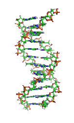
2005: Erik Winfree and Paul Rothemund from the California Institute of Technology developed theories for DNA-based computation and algorithmic self-assembly in which computations are embedded in the process of nanocrystal growth.
2006: James Tour and colleagues at Rice University built a nanoscale car made of oligo(phenylene ethynylene) with alkynyl axles and four spherical C60 fullerene (buckyball) wheels. In response to increases in temperature, the nanocar moved about on a gold surface as a result of the buckyball wheels turning, as in a conventional car. At temperatures above 300C it moved around too fast for the chemists to keep track of it! (Image at left.)
2007: Angela Belcher and colleagues at MIT built a lithium-ion battery with a common type of virus that is nonharmful to humans, using a low-cost and environmentally benign process. The batteries have the same energy capacity and power performance as state-of-the-art rechargeable batteries being considered to power plug-in hybrid cars, and they could also be used to power personal electronic devices. (Image at right.)
2008: The first official NNI Strategy for Nanotechnology-Related Environmental, Health, and Safety (EHS) Research was published, based on a two-year process of NNI-sponsored investigations and public dialogs. This strategy document was updated in 2011, following a series of workshops and public review.
20092010: Nadrian Seeman and colleagues at New York University createdseveral DNA-like robotic nanoscale assembly devices.One is a process for creating 3D DNA structures using synthetic sequences of DNA crystals that can be programmed to self-assemble using sticky ends and placement in a set order and orientation.Nanoelectronics could benefit:the flexibility and density that 3D nanoscale components allow could enable assembly of parts that are smaller, more complex, and more closely spaced. Another Seeman creation (with colleagues at Chinas Nanjing University) is a DNA assembly line. For this work, Seeman shared the Kavli Prize in Nanoscience in 2010.
2010: IBM used a silicon tip measuring only a few nanometers at its apex (similar to the tips used in atomic force microscopes) to chisel away material from a substrate to create a complete nanoscale 3D relief map of the world one-one-thousandth the size of a grain of saltin 2 minutes and 23 seconds. This activity demonstrated a powerful patterning methodology for generating nanoscale patterns and structures as small as 15 nanometers at greatly reduced cost and complexity, opening up new prospects for fields such as electronics, optoelectronics, and medicine. (Image below.)
2011:The NSET Subcommittee updated both the NNI Strategic Plan and the NNI Environmental, Health, and Safety Research Strategy, drawing on extensive input from public workshops and online dialog with stakeholders from Government, academia, NGOs, and the public, and others.
2012: The NNI launched two more Nanotechnology Signature Initiatives (NSIs)--Nanosensors and the Nanotechnology Knowledge Infrastructure (NKI)--bringing the total to five NSIs.
2013: -The NNI starts the next round of Strategic Planning, starting with the Stakeholder Workshop. -Stanford researchers develop the first carbon nanotube computer.
2014: -The NNI releases the updated 2014 Strategic Plan. -The NNI releases the 2014 Progress Review on the Coordinated Implementation of the NNI 2011 Environmental, Health, and Safety Research Strategy.
Go here to read the rest:
Nanotechnology Timeline | National Nanotechnology Initiative
- Carla wants to know [Last Updated On: November 7th, 2010] [Originally Added On: November 7th, 2010]
- Carla wants to know [Last Updated On: November 7th, 2010] [Originally Added On: November 7th, 2010]
- I believe in Renewable Energy, and here's why [Last Updated On: May 8th, 2011] [Originally Added On: May 8th, 2011]
- I believe in Renewable Energy, and here's why [Last Updated On: May 8th, 2011] [Originally Added On: May 8th, 2011]
- U.S. and Canadian Scientists Form a Global Alliance for Nano-Bio-Electronics in Order to Rapidly Find Solutions for ... [Last Updated On: February 13th, 2012] [Originally Added On: February 13th, 2012]
- Regenerative Medicine Biotech Company, Eqalix, Names Scientific Advisory Board [Last Updated On: October 9th, 2012] [Originally Added On: October 9th, 2012]
- Welcome to the body parts shop... would you like to place an order? [Last Updated On: April 15th, 2014] [Originally Added On: April 15th, 2014]
- Stem cells hold keys to body's plan [Last Updated On: June 6th, 2014] [Originally Added On: June 6th, 2014]
- InVivo Therapeutics [Last Updated On: November 12th, 2014] [Originally Added On: November 12th, 2014]
- Nanobiotechnology - Wikipedia, the free encyclopedia [Last Updated On: October 1st, 2015] [Originally Added On: October 1st, 2015]
- Center for Drug Delivery and Nanomedicine (CDDN) [Last Updated On: October 8th, 2015] [Originally Added On: October 8th, 2015]
- Nanomedicine: Nanotechnology, Biology and Medicine ... [Last Updated On: October 20th, 2016] [Originally Added On: October 20th, 2016]
- Nanobiotechnology - Wikipedia [Last Updated On: November 19th, 2016] [Originally Added On: November 19th, 2016]
- Exploiting acidic tumor microenvironment for the development of novel cancer nano-theranostics - Medical Xpress [Last Updated On: July 6th, 2017] [Originally Added On: July 6th, 2017]
- Nano-sized drug carriers could be the future for patients with lung disease - Phys.Org [Last Updated On: July 6th, 2017] [Originally Added On: July 6th, 2017]
- Nano Medicine [Last Updated On: July 6th, 2017] [Originally Added On: July 6th, 2017]
- Healthcare Nanotechnology (Nanomedicine) Market Expected to Generate Huge Profits by 2015 2021: Persistence ... - MilTech [Last Updated On: July 6th, 2017] [Originally Added On: July 6th, 2017]
- Nanomedicine Research Journal [Last Updated On: September 25th, 2017] [Originally Added On: September 25th, 2017]
- Top Nanomedicine Conferences|DrugDelivery meetings ... [Last Updated On: June 29th, 2018] [Originally Added On: June 29th, 2018]
- The Promise of Nanomedicine - Laboratory Equipment [Last Updated On: July 23rd, 2018] [Originally Added On: July 23rd, 2018]
- Nanomedicine Conferences | Nanotechnology Events ... [Last Updated On: October 8th, 2018] [Originally Added On: October 8th, 2018]
- Nanomedicine - Overview [Last Updated On: October 8th, 2018] [Originally Added On: October 8th, 2018]
- IEEE-NANOMED 2016 The 10th IEEE International Conference ... [Last Updated On: October 13th, 2018] [Originally Added On: October 13th, 2018]
- Journal of Nanomedicine and Biotherapeutic Discovery- Open ... [Last Updated On: May 1st, 2019] [Originally Added On: May 1st, 2019]
- Nano-biotechnology Market by Manufacturer Analysis 2016-2024 - BitGmx [Last Updated On: September 22nd, 2019] [Originally Added On: September 22nd, 2019]
- Growing hair on bald heads with electric tech may soon be easy - Livemint [Last Updated On: September 22nd, 2019] [Originally Added On: September 22nd, 2019]
- Global Nanorobots Market Prospective Growth, Opportunities, Top Key Players and Forecast to 2024 - Pioneer Reporter [Last Updated On: September 22nd, 2019] [Originally Added On: September 22nd, 2019]
- Nanotechnology in Medical Applications Market: Strategic Analysis to Understand the Competitive Outlook of the Industry, 2025 - Market Forecast [Last Updated On: September 22nd, 2019] [Originally Added On: September 22nd, 2019]
- Functional Polymer Market Insights, Trends, Analysis, Types, Applications, key players, Market shares and Forecast 2019 to 2027 - The Market Plan [Last Updated On: September 22nd, 2019] [Originally Added On: September 22nd, 2019]
- Healthcare Nanotechnology (Nanomedicine) Market to Witness Growth Acceleration During 2015 2021 - Trading Herald [Last Updated On: September 22nd, 2019] [Originally Added On: September 22nd, 2019]
- Curcumin hope in TB fight - Telegraph India [Last Updated On: September 22nd, 2019] [Originally Added On: September 22nd, 2019]
- TB vaccines with nano-curcumin work wonders - Deccan Herald [Last Updated On: September 22nd, 2019] [Originally Added On: September 22nd, 2019]
- Healthcare Nanotechnology (Nanomedicine) Market Likely To Experience High Revenue Generation In The Forthcoming Years - Commerce Gazette [Last Updated On: September 22nd, 2019] [Originally Added On: September 22nd, 2019]
- Healthcare Nanotechnology Nanomedicine Market to Witness a Pronounce Growth During 2019-2029 - Zebvo [Last Updated On: September 22nd, 2019] [Originally Added On: September 22nd, 2019]
- Self-Assembly Of Retinoid Nanoparticles For Melanoma Therapy | IJN - Dove Medical Press [Last Updated On: October 5th, 2019] [Originally Added On: October 5th, 2019]
- Improving 131I Radioiodine Therapy By Hybrid Polymer-Grafted Gold Nano | IJN - Dove Medical Press [Last Updated On: October 5th, 2019] [Originally Added On: October 5th, 2019]
- Nanorobotic Market 2019 Technological Perspective, Latest Trends and key manufacturers:: Bruker, Jeol, Thermo Fisher Scientific, Ginkgo Bioworks -... [Last Updated On: October 22nd, 2019] [Originally Added On: October 22nd, 2019]
- Quantum dots that light up TVs could be used for brain research - Stuff Magazines [Last Updated On: October 22nd, 2019] [Originally Added On: October 22nd, 2019]
- 4 Innovative Solutions Fostering Advanced Cancer Treatment - Medical Tech Outlook [Last Updated On: October 28th, 2019] [Originally Added On: October 28th, 2019]
- Nanotechnology for disease diagnosis and treatment earns Florida Poly professor international award - Yahoo Finance [Last Updated On: November 19th, 2019] [Originally Added On: November 19th, 2019]
- Nanorobotics Market analysis and outlook for 2019-202 available in the latest report - WhaTech - WhaTech [Last Updated On: November 21st, 2019] [Originally Added On: November 21st, 2019]
- Global Next-Generation Sequencing (NGS) Market Report 2019 - World Market Projected to Surpass $25 Billion by 2026, Rising at a CAGR of 20.6% -... [Last Updated On: November 21st, 2019] [Originally Added On: November 21st, 2019]
- World Pancreatic Cancer Day: increasing awareness and inspiring action - UNSW Newsroom [Last Updated On: November 21st, 2019] [Originally Added On: November 21st, 2019]
- NanoRobotics Market Overview on Future Threats by 2026 - Crypto News Byte [Last Updated On: November 25th, 2019] [Originally Added On: November 25th, 2019]
- Nanoparticle therapy shows promise for treatment of rare cancer - The Brown Daily Herald [Last Updated On: November 25th, 2019] [Originally Added On: November 25th, 2019]
- What is the Role of Nanomedicine in Treating Melanoma? - Medical Tech Outlook [Last Updated On: January 2nd, 2020] [Originally Added On: January 2nd, 2020]
- Our top 20 features of 2019 - COVER [Last Updated On: January 5th, 2020] [Originally Added On: January 5th, 2020]
- Examine Triple Negative Breast Cancer Treatment Market expected to reach US$ 720 mn by 2026 - WhaTech Technology and Markets News [Last Updated On: January 10th, 2020] [Originally Added On: January 10th, 2020]
- Triple Negative Breast Cancer Treatment Market Combining Therapies - Communal News [Last Updated On: January 10th, 2020] [Originally Added On: January 10th, 2020]
- A Chelate-Free Nano-Platform for Incorporation of Diagnostic and Thera | IJN - Dove Medical Press [Last Updated On: January 10th, 2020] [Originally Added On: January 10th, 2020]
- VVUS Stock Jumps 70% on FDA Nod for New Formulation of Pancreaze - MicroSmallCap [Last Updated On: February 6th, 2020] [Originally Added On: February 6th, 2020]
- Is the Lieber Arrest Linked to Military Brain Research and China? - Bryen's Blog [Last Updated On: February 6th, 2020] [Originally Added On: February 6th, 2020]
- The Future Of Nano Medicine [Last Updated On: February 6th, 2020] [Originally Added On: February 6th, 2020]
- Nano Medicine: Meaning, Advantages and Disadvantages [Last Updated On: February 6th, 2020] [Originally Added On: February 6th, 2020]
- Immix Doses First Patient in USA in its Phase 1b/2a Trial in Patients with Advanced Solid Tumors - BioSpace [Last Updated On: February 11th, 2020] [Originally Added On: February 11th, 2020]
- Kanazawa University Research: Combined Drug Treatment for Lung Cancer and Secondary Tumors - Yahoo Finance [Last Updated On: February 11th, 2020] [Originally Added On: February 11th, 2020]
- Edited Transcript of NANO earnings conference call or presentation 6-Feb-20 9:30pm GMT - Yahoo Finance [Last Updated On: February 11th, 2020] [Originally Added On: February 11th, 2020]
- All your questions about how to wear a face mask -- answered - Action News Now [Last Updated On: April 26th, 2020] [Originally Added On: April 26th, 2020]
- The future of medicine - Switzer Financial News [Last Updated On: May 10th, 2020] [Originally Added On: May 10th, 2020]
- Recent Progress and Future Directions: The Nano-Drug Delivery System f | IJN - Dove Medical Press [Last Updated On: May 10th, 2020] [Originally Added On: May 10th, 2020]
- Inolife is going to revolutionize how we take our medicine - BNNBloomberg.ca [Last Updated On: May 24th, 2020] [Originally Added On: May 24th, 2020]
- Evergreen Medical Acupuncture is now offering its own supplement and herbal products, Dr. Ficks Functional Farmacy! - TippNews DAILY [Last Updated On: June 10th, 2020] [Originally Added On: June 10th, 2020]
- Impact of Covid-19 on Nano Chemotherapy Market is Expected to Grow at an active CAGR by Forecast to 2026 | Top Players Dell Wyse, IBM, Microsoft -... [Last Updated On: June 15th, 2020] [Originally Added On: June 15th, 2020]
- Kanazawa University Research: Cell Removal as the Result of a Mechanical Instability - PR Newswire UK [Last Updated On: June 15th, 2020] [Originally Added On: June 15th, 2020]
- Coronavirus threat to global Healthcare Nanotechnology (Nanomedicine) Market 2020 Industry Share, Size, Consumption, Growth, Top Manufacturers, Type... [Last Updated On: June 15th, 2020] [Originally Added On: June 15th, 2020]
- Nanocellulose Market to Reach USD 1.08 Billion by 2027 | CAGR:20.4% | Reports And Data - PRNewswire [Last Updated On: June 17th, 2020] [Originally Added On: June 17th, 2020]
- Cellics Therapeutics Announces the Publication of Cellular Nanosponges Inhibit SARS-CoV-2 Infectivity in Nano Letters - BioSpace [Last Updated On: June 17th, 2020] [Originally Added On: June 17th, 2020]
- Opportunities in the World Nanotechnology Market to 2025 - Application of Nanotechnology in Wastewater Treatment and Enhanced Renewable Energy Driving... [Last Updated On: August 12th, 2020] [Originally Added On: August 12th, 2020]
- Interview: The NDB team on its revolutionary nano-diamond batteries - New Atlas [Last Updated On: August 29th, 2020] [Originally Added On: August 29th, 2020]
- What is Nanoscience? | Outlook and How to Invest | INN - Investing News Network [Last Updated On: September 23rd, 2020] [Originally Added On: September 23rd, 2020]
- Global Nano Therapy Market- Industry Analysis and Forecast (2020-2027) - Stock Market Vista [Last Updated On: October 29th, 2020] [Originally Added On: October 29th, 2020]
- Nanox Signs With Ambra Health to Enable Image Access and Transfer with US Hospitals and Medical imaging Providers - BioSpace [Last Updated On: October 31st, 2020] [Originally Added On: October 31st, 2020]
- Global Nanobots Market 2020 | Research Report Covers | (COVID-19 Analysis) | Industry Research, Drivers, Top Trends | Global Analysis And Forecast to... [Last Updated On: October 31st, 2020] [Originally Added On: October 31st, 2020]
- Thomas Jefferson Awards Highlight Research and Service to the University - UVA Today [Last Updated On: June 6th, 2021] [Originally Added On: June 6th, 2021]
- The Future of Cancer Treatment Using Nanotechnology - AZoNano [Last Updated On: June 6th, 2021] [Originally Added On: June 6th, 2021]
- Nanomedicine is transforming healthcare innovation - Korea IT Times [Last Updated On: June 6th, 2021] [Originally Added On: June 6th, 2021]
- Nanomedicine in Central Nervous System Injury and Repair Market Report- Trends Key Programs Analysis and Competitive Landscape Analysis The Manomet... [Last Updated On: June 23rd, 2021] [Originally Added On: June 23rd, 2021]
- Matrix Meats Adds to Team as Interest in Cultivated Meat Grows - PRNewswire [Last Updated On: July 21st, 2021] [Originally Added On: July 21st, 2021]
- Biodistribution of sphingolipid nanoemulsions with 68Ga | IJN - Dove Medical Press [Last Updated On: August 31st, 2021] [Originally Added On: August 31st, 2021]
- 2009 show based on conspiracy theories is shared as proof of WHO working on COVID-19 vaccines to create permanent sterility - Factly [Last Updated On: January 5th, 2022] [Originally Added On: January 5th, 2022]